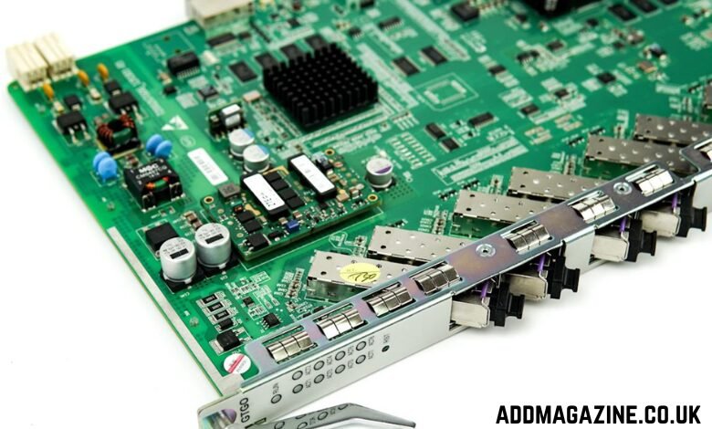
In electronics, there’s a moment where things quietly change. Signals stop behaving like polite messengers and start acting more like waves with opinions of their own. That’s usually the point where standard circuit board thinking no longer works — and where high-frequency PCB enters the conversation.
If you’ve ever dealt with RF modules, 5G hardware, aerospace electronics, or fast digital systems that push into the gigahertz range, you already know the feeling. The board that looked perfect on paper suddenly introduces noise, signal loss, or timing problems you didn’t budget for. Traces become transmission lines. Copper geometry matters. Even the laminate starts to have a personality.
This article is a practical, experience-driven look at high-frequency PCBs — not just what they are, but how they behave in the real world, how they’re manufactured, and why choosing the right fabrication partner (including specialists like FastTurn PCB) makes a measurable difference.
Let’s slow it down, break it apart, and talk honestly about what matters.
What Is a High-Frequency PCB, Really?
On paper, a high-frequency PCB is usually defined by operating frequencies above 500 MHz, and more commonly above 1 GHz. But that definition barely scratches the surface.
The truth is, frequency alone doesn’t tell the full story.
A board carrying a 3 GHz signal over a few millimeters behaves very differently from one routing that same signal across multiple layers, connectors, and vias. What makes a PCB “high-frequency” isn’t just the number — it’s how sensitive the signal becomes to the physical environment around it.
At high frequencies:
- Traces act like controlled-impedance transmission lines
- Dielectric constant variations start affecting timing
- Copper surface roughness contributes to loss
- Crosstalk increases dramatically
- Power and ground planes must behave predictably
In other words, the PCB stops being a neutral platform and becomes an active part of the circuit.
That’s why high-frequency design isn’t a niche skill — it’s a mindset shift.
Why High-Frequency PCBs Matter More Than Ever
Ten years ago, RF boards lived mostly in telecom racks and defense systems. Today, they’re everywhere.
You’ll find high-frequency PCBs in:
- 5G and wireless infrastructure
- Automotive radar and ADAS systems
- Medical imaging and diagnostic devices
- Aerospace navigation and communication
- High-speed data centers
- IoT gateways and edge devices
Even consumer electronics now push signal speeds that would’ve been considered extreme not long ago.
At the same time, expectations haven’t softened. Devices still need to be smaller, lighter, cheaper, and more reliable — often all at once.
That combination is why high-frequency PCB manufacturing has become one of the most demanding segments of electronics production.
The Core Challenges of High-Frequency PCB Design
Let’s be honest — most issues with high-frequency boards don’t come from bad schematics. They come from underestimating physics.
Signal Integrity Is the Main Event
At high frequencies, signal integrity isn’t something you “optimize later.” It’s the foundation.
Small discontinuities in trace width, impedance mismatches, or poorly placed vias can cause:
- Reflections
- Attenuation
- Phase distortion
- Eye diagram collapse
You may not see it on a multimeter, but oscilloscopes and network analyzers will tell the story quickly.
Dielectric Properties Aren’t Optional Knowledge
FR-4 works beautifully for many designs. But once you’re deep into RF or microwave territory, its dielectric constant variability becomes a liability.
High-frequency laminates are chosen for:
- Stable dielectric constant (Dk)
- Low dissipation factor (Df)
- Consistent performance across temperature
Ignoring these parameters is one of the fastest ways to introduce unpredictable behavior.
Layout Decisions Carry More Weight
At low frequencies, routing is forgiving. At high frequencies, every decision compounds.
- Trace length matching becomes critical
- Sharp corners introduce impedance discontinuities
- Via stubs can act like antennas
- Ground return paths must be intentional
This is where experience really shows.
Materials Used in High-Frequency PCBs
Material selection is where many high-frequency projects either succeed quietly or struggle loudly.
Common High-Frequency Substrates
Some of the most widely used materials include:
- Rogers laminates (RO4000, RO3000 series)
- Taconic materials
- Isola high-speed laminates
- PTFE-based substrates
Each comes with trade-offs in cost, machinability, thermal performance, and frequency response.
Copper Matters More Than You Think
At high frequencies, current flows primarily on the surface of the conductor — the skin effect. That makes copper roughness a real contributor to signal loss.
Many high-frequency PCBs use:
- Rolled annealed copper
- Smooth copper foils
- Low-profile or very-low-profile copper
It’s a small detail that adds up quickly at scale.
Manufacturing Tolerances and Why They’re Tighter
Designing a high-frequency PCB is only half the challenge. Manufacturing it correctly is the other half — and often the harder one.
Controlled Impedance Isn’t a Suggestion
Impedance control must be precise. A few ohms off can degrade performance significantly.
This requires:
- Tight control of trace width and spacing
- Accurate dielectric thickness
- Consistent lamination processes
- Verification through impedance testing
Not every PCB shop is equipped — or willing — to hold those tolerances.
Registration and Layer Alignment
Multi-layer high-frequency boards rely heavily on proper layer-to-layer alignment.
Misregistration can:
- Change effective impedance
- Introduce skew
- Increase crosstalk
These aren’t cosmetic defects. They directly affect performance.
Clean Fabrication Environment
High-frequency materials can be more sensitive during processing. Dust, moisture, or improper handling can introduce defects that don’t show up until testing — or worse, in the field.
That’s why specialized manufacturers like FastTurn PCB are often chosen for RF and high-speed projects. They’re built around these constraints, not adapting to them after the fact.
Prototyping vs. Production: Different Pressures, Same Physics
One of the quiet challenges in high-frequency PCB work is the transition from prototype to production.
A prototype may work perfectly at small volumes, but scaling it introduces new variables:
- Material availability changes
- Process windows tighten
- Cost pressure increases
- Yield becomes critical
Fast-turn prototypes are valuable, but they need to be representative of production conditions. Otherwise, you’re validating the wrong thing.
Why Turnaround Time Still Matters in High-Frequency Projects
It’s easy to assume that high-frequency boards must always move slowly. Careful work takes time, after all.
But development cycles don’t pause just because physics is complicated.
Engineers still need:
- Rapid iteration
- Design validation
- Signal integrity testing
- Early field trials
Fast, reliable fabrication enables better decisions earlier in the process. It reduces guesswork and accelerates learning.
That balance — speed without cutting corners — is difficult, but not impossible.
Testing and Validation of High-Frequency PCBs
Testing high-frequency boards isn’t casual work.
Common validation methods include:
- Time-domain reflectometry (TDR)
- Vector network analysis (VNA)
- Eye diagram analysis
- S-parameter measurement
These tests don’t just confirm functionality — they reveal margin. And margin is what keeps products stable across temperature, aging, and manufacturing variation.
The Role of the PCB Manufacturer in High-Frequency Success
Let’s be honest — not all PCB manufacturers are created equal, especially when it comes to RF and high-speed work.
A capable high-frequency PCB manufacturer offers more than fabrication:
- Material guidance
- Stackup recommendations
- DFM feedback
- Controlled impedance validation
- Consistent process control
Companies like FastTurn PCB position themselves as technical partners, not just order takers — and that mindset shows in the final product.
Where High-Frequency PCB Technology Is Headed
The demand curve isn’t flattening.
As systems push higher data rates and frequencies, we’ll see:
- More hybrid stackups (RF + digital)
- Tighter impedance tolerances
- Increased use of simulation-driven design
- Greater collaboration between designers and fabricators
High-frequency PCBs won’t become easier — but they will become more central.
Choosing the Right Partner for High-Frequency PCB Fabrication
So how do you choose?
Ask practical questions:
- Do they regularly work with RF materials?
- Can they demonstrate impedance control capability?
- How do they handle fast-turn prototypes?
- Do they provide engineering feedback?
If the answers feel vague, that’s usually a signal in itself.
Working with specialists like FastTurn PCB often shortens development cycles simply because fewer assumptions are made — and fewer surprises appear later.
Final Thoughts: High Frequency Rewards Respect
High-frequency PCB design and manufacturing reward teams who respect the physics, plan carefully, and collaborate early.
There’s no shortcut that replaces experience, but there are partners and processes that make the journey smoother.
When signals move faster, mistakes get louder. When boards are built right, though, everything just works — quietly, predictably, and reliably.
And honestly, that’s the goal.


