Morgen Dautrich is a name synonymous with innovation and expertise in the semiconductor industry. As a professional with an educational background in Applied Physics and Material Engineering from Penn State University, Dautrich has contributed significantly to the field through hands-on experimental work, research collaborations, and advanced knowledge in atomic-scale defects in semiconductor devices. His research focuses on using cutting-edge techniques to study and improve the functionality of semiconductors, particularly in the context of silicon carbide (SiC) devices used in power electronics.
This post takes a detailed look at Dautrich’s academic background, professional journey, and contributions to the semiconductor industry, offering insight into his career, key achievements, and the technologies he has worked with.
Early Education and Academic Background
Morgen Dautrich’s academic journey began at Penn State University, where he earned his Master of Science (MS) degree in Applied Physics and Material Engineering between 1998 and 2006. During his time at Penn State, Dautrich was not only an excellent student but also highly engaged in extracurricular activities. He was a member of the Eta Kappa Nu (EE Honor Society), and his active participation in the university’s research ecosystem helped him achieve 1st place in the Engineering Science and Mechanics (ESM) Research Symposium in 2006. His involvement in various activities like the Engineering Mentorship Program and Project WISE further enhanced his technical and leadership skills.
Dautrich’s master’s research was conducted under the mentorship of Professor P.M. Lenahan in the Department of Engineering Science & Mechanics, which focused on understanding and addressing atomic-scale defects in semiconductor devices, a key aspect of advancing technology in the semiconductor industry. During this time, he also developed hands-on expertise in using magnetic resonance techniques, including electron spin resonance (ESR) and spin-dependent recombination, to study these defects. His research also involved the use of standard electrical measurements, laying the foundation for his future work in semiconductor device optimization.
Specialization in Semiconductor Devices
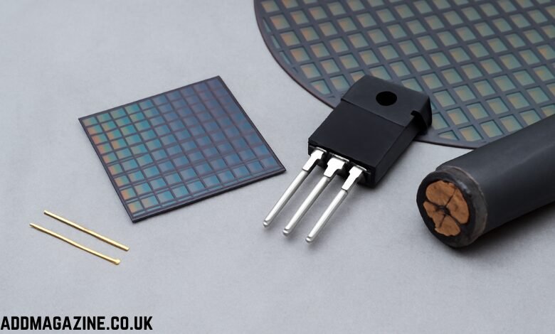
Dautrich’s research focused on semiconductors, specifically materials like 4H and 6H-Silicon Carbide (SiC), which are widely used in the manufacturing of high-power and high-temperature electronic devices such as metal-oxide-semiconductor field-effect transistors (MOSFETs). Silicon carbide is a material of choice for power electronics due to its ability to withstand higher voltages, temperatures, and frequencies compared to traditional silicon.
One of Dautrich’s notable achievements was his collaboration with prestigious organizations like the Army Research Labs and CREE Inc., a leading developer of silicon carbide technologies. His research efforts in identifying deep-level defects in state-of-the-art SiC MOSFETs were critical in pushing the boundaries of power electronics. The identification of such defects is essential in improving the performance and reliability of these devices, which are used in applications ranging from automotive to energy systems.
Dautrich’s hands-on experimental work included the use of advanced magnetic resonance techniques like electron spin resonance (ESR) and spin-dependent recombination, which allow for the study of the fundamental atomic-level behavior of semiconductors. This research methodology has been pivotal in understanding how atomic-scale defects affect the performance of semiconductor devices and in developing strategies to mitigate these defects.
Professional Experience and Contributions
Morgen Dautrich’s academic prowess translated seamlessly into his professional career. He has spent several years working in the semiconductor industry, where he has gained significant expertise in materials engineering, defect analysis, and device optimization. His work has focused on the experimental study of atomic-scale defects, which play a crucial role in the overall efficiency of semiconductor devices.
Dautrich’s collaboration with Army Research Labs and CREE Inc. stands as a testament to his role in advancing semiconductor technology. These partnerships were crucial in identifying key challenges faced by SiC MOSFETs and creating solutions that can enhance their efficiency and durability. Through his work, Dautrich has helped ensure that semiconductor devices, particularly those designed for high-power applications, are optimized for real-world use, ensuring better performance and reliability.
His research contributions extend beyond just understanding semiconductor materials; Dautrich has also focused on improving the processes used in semiconductor manufacturing. This includes chemical safety training, manual wire bonding, and various other technical skills that are integral to the semiconductor manufacturing process. His practical skills, combined with his theoretical knowledge, have made him a highly sought-after professional in the field.
Achievements and Recognition
Morgen Dautrich’s achievements in the semiconductor field have earned him widespread recognition. His win at the 2006 Engineering Science and Mechanics (ESM) Research Symposium was a significant milestone in his academic career, where he presented groundbreaking work on semiconductor defects. This early recognition helped propel him into the semiconductor industry, where his hands-on research and collaboration with industry leaders continued to shape his career.
Furthermore, Dautrich’s contributions to the development of high-efficiency SiC MOSFETs have had a lasting impact on the field of power electronics. These devices are essential for modern technologies such as electric vehicles, renewable energy systems, and industrial applications. The ability to improve the performance of these devices has profound implications for energy efficiency and sustainability, making Dautrich’s work not only technically significant but also environmentally impactful.
Legacy and the Future of Semiconductor Engineering
As the semiconductor industry continues to evolve, professionals like Morgen Dautrich will remain at the forefront of innovation. With the increasing demand for energy-efficient and high-performance electronic devices, the role of semiconductor engineers becomes ever more critical. Dautrich’s work in studying atomic-scale defects and improving the design and manufacturing of SiC MOSFETs will play a pivotal role in shaping the future of semiconductor technology.
Looking forward, Dautrich’s ongoing research and expertise in semiconductor materials engineering will likely continue to influence the development of next-generation semiconductor devices. As power electronics become increasingly integral to a wide range of industries, from automotive to energy to telecommunications, professionals like Dautrich will be crucial in ensuring that these devices meet the rigorous demands of modern applications.
Conclusion
Morgen Dautrich’s career is a perfect example of how academic excellence, hands-on research, and collaboration with industry leaders can lead to groundbreaking contributions in the field of semiconductor technology. From his early days at Penn State University to his current work in the semiconductor industry, Dautrich has continuously pushed the boundaries of what is possible in the field of materials engineering. His expertise in studying atomic-scale defects in semiconductors has helped drive the development of more efficient and reliable power electronics, which are central to a wide range of modern technologies.
As the semiconductor industry continues to grow and evolve, Morgen Dautrich’s work will undoubtedly have a lasting impact. His contributions to the field of material engineering, particularly in relation to SiC MOSFETs, have positioned him as a key figure in the ongoing development of high-performance electronic devices that are essential for a sustainable future.